1 暨南大学信息科学技术学院,广东 广州 510632
2 上海交通大学区域光纤通信网与新型光通信系统国家重点实验室,上海 200240
硅基微环谐振器由于其优异的光谱选择性、紧凑的占地面积和低功耗特性,被大量应用于光子集成领域。但是,由制造误差和硅基器件高热敏性引起的微环谐振波长偏移会导致工作状态不稳定,在实际应用中需要实现相应的波长锁定方案。提出了一种基于差分进化和数字微扰的微环波长锁定系统,以输出光功率为监测变量,在全局搜索阶段基于差分进化算法搜索最佳加热功率来定位目标信号波长,在局部锁定阶段基于数字微扰算法解调出误差信号,据此来增减加热功率以消除环境温度波动干扰。经过理论推导和实验验证,发现提出的差分进化算法搜索最佳加热功率的速度比传统的逐步扫描方式快4倍左右,实验验证了在400 s内、在环境温度变化5 ℃条件下微环谐振波长的稳定锁定。
硅基微环 波长锁定 差分进化 数字微扰 激光与光电子学进展
2023, 60(23): 2323002
1 State Key Lab of Advanced Optical Communication Systems and Networks, Department of Electronic Engineering, Shanghai Jiao Tong University, Shanghai 200240, China
2 Institute of Microelectronics and Key Laboratory for Magnetism and Materials of Ministry of Education, School of Physical Science and Technology, Lanzhou University, Lanzhou 730000, China
Frontiers of Optoelectronics
2022, 15(1): s12200
上海交通大学 区域光纤通信网与新型光通信系统国家重点实验室, 上海 200240
针对微环谐振器用于折射率传感时动态范围较窄的问题, 提出了一种基于少模氮化硅微环谐振器的折射率传感技术, 使谐振波长漂移的计算能够不用考虑原始参考值以及增大折射率探测范围, 并验证高阶模对环境变化更敏感。通过理论分析, 建立仿真模型, 验证了该方法的可行性, 并使用具有不同折射率的待测溶液开展传感实验, 得到了91.79 nm/RIU的折射率灵敏度与10-5 RIU的分辨率。
微环谐振器 折射率传感器 氮化硅波导 micro-ring resonator refractive index sensor silicon nitride waveguide
Author Affiliations
Abstract
State Key Laboratory of Advanced Optical Communication Systems and Networks, Department of Electronic Engineering, Shanghai Jiao Tong University, Shanghai 200240, China
We experimentally demonstrate high-efficiency and broadband four-wave mixing in a silicon-graphene strip waveguide. A four-wave mixing conversion efficiency of 38.7 dB and a 3-dB conversion bandwidth of 35 nm are achieved in the silicon-graphene strip waveguide with an optimized light-graphene interaction length of 60 μm. The interaction length is controlled by a windowed area of silica layer on the silicon waveguide. Numerical simulations and experimental studies are carried out and show a nonlinear parameter γGOS as large as 104 W 1 ·m 1.
Integrated optics devices Nonlinear optics, four-wave mixing Nonlinear optical materials Photonics Research
2018, 6(10): 10000965
Author Affiliations
Abstract
State Key Laboratory of Advanced Optical Communication Systems and Networks, Department of Electronic Engineering, Shanghai Jiao Tong University, Shanghai 200240, China
In this paper, we review our recent work on thermo-optic all-optical devices based on two-dimensional (2D) materials. The unique properties of 2D materials enable fast and highly efficient thermo-optic control of light. A few all-optical devices are demonstrated based on various thermo-optic mechanisms. Both fiber and integrated devices will be shown.
Nanomaterials All-optical devices Integrated optics devices Photonics Research
2018, 6(10): 10000C22
State Key Lab of Advanced Optical Communication Systems and Networks, Department of Electronic Engineering,Shanghai Jiao Tong University, Shanghai 200240, China
Frontiers of Optoelectronics
2018, 11(1): 0177
Author Affiliations
Abstract
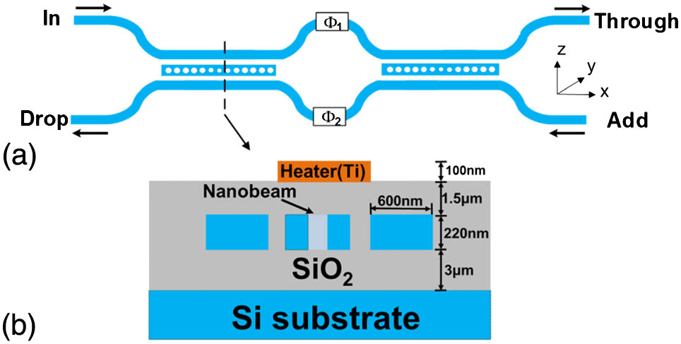
1 State Key Lab of Advanced Optical Communication Systems and Networks, Department of Electronic Engineering, Shanghai Jiao Tong University, Shanghai 200240, China
2 Engineering Department, University of Massachusetts, Boston, Massachusetts 02125, USA
3 e-mail: qiuciyuan@sjtu.edu.cn
4 e-mail: yikaisu@sjtu.edu.cn
We propose and experimentally demonstrate a 2×2 thermo-optic (TO) crossbar switch implemented by dual photonic crystal nanobeam (PCN) cavities within a silicon-on-insulator (SOI) platform. By thermally tuning the refractive index of silicon, the resonance wavelength of the PCN cavities can be red-shifted. With the help of the ultrasmall mode volumes of the PCN cavities, only ~0.16 mW power is needed to change the switching state. With a spectral passband of 0.09 nm at the 1583.75 nm operation wavelength, the insertion loss (IL) and crosstalk (CT) performances were measured as IL(bar)= 0.2 dB, CT(bar)= 15 dB, IL(cross)= 1.5 dB, and CT(cross)= 15 dB. Furthermore, the thermal tuning efficiency of the fabricated device is as high as 1.23 nm/mW.
Integrated optics devices Photonic crystals Optical switching devices Photonics Research
2017, 5(2): 02000108

Author Affiliations
Abstract
State Key Lab of Advanced Optical Communication Systems and Networks, Department of Electronic Engineering, Shanghai Jiao Tong University, Shanghai 200240, China
Mode- and polarization-division multiplexing offer new dimensions to increase the transmission capacity of optical communications. Selective switches are key components in reconfigurable optical network nodes. An on-chip silicon 2×2 mode- and polarization-selective switch that can route four data channels on two modes and two polarizations simultaneously is proposed and experimentally demonstrated for the first time, to the best of our knowledge. The overall insertion losses are lower than 8.6 dB. To reduce the inter-modal crosstalk, polarization beam splitters are added to filter the undesired polarizations or modes. The measured inter-modal and intra-modal crosstalk values are below ?23.2 and ?22.8 dB for all the channels, respectively.
(130.3120) Integrated optics devices (060.4230) Multiplexing (130.4815) Optical switching devices. Photonics Research
2017, 5(5): 05000521
Author Affiliations
Abstract
1 State Key Laboratory of Advanced Optical Communication Systems and Networks, Department of Electronic Engineering, Shanghai Jiao Tong University, Shanghai 200240, China
2 Laboratoire de technologies de réseaux, école de technologie supérieure, Montreal, Canada
We propose and experimentally demonstrate compact on-chip 1 × 2 wavelength selective switches (WSSs) based on silicon microring resonators (MRRs) with nested pairs of subrings (NPSs). Owing to the resonance splitting induced by the inner NPSs, the proposed devices are capable of performing selective channel routing at certain resonance wavelengths of the outer MRRs. System demonstration of dynamic channel routing using fabricated devices with one and two NPSs is carried out for 10 Gb∕s non-return-to-zero signal. The experimental results verify the effectiveness of the fabricated devices as compact on-chip WSSs.
Integrated optics devices Resonators Optical switching devices Photonics Research
2015, 3(1): 01000009


